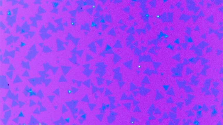
CVD grown monolayer MoS₂ crystals on a Si wafer
Date: 16.11.2021
Time: 14:00 - 17:00 Uhr
Participation: Online
Zoom
Languages: German/English
Due to the novelty of 2D materials, their reproducible and large-scale production is remaining a central challenge for their use in industry at present. Worldwide and within the 2D-Mat-Net, there is a great interest in research and development of methods for top-down and bottom-up fabrication of 2D materials both in academic and industrial environment.
In this workshop, the production of 2D materials for different applications, e.g., electronics, photonics, energy storage, energy conversion, medicine, etc. will be presented. Moreover, the potential of 2D materials for implementation in functional coatings is discussed.
You can register hereExternal link. Participation is free of charge.
| Time | Program |
| 13:45 | Opening of the virtual conference room |
| 14:00 | Welcome |
| 14:05 | Use of graphene for improving corrosion resistance in protective coatings Dr. Karanveer Aneja, Talga Group Ltd. |
| 14:35 | Processable and easy-to-use, in-situ functionalized graphenes via electrochemical exfoliation Dr. Martin R. Lohe, Sixonia Tech GmbH |
| 15:05 | Production of 2D nanosheets in the liquid phase Prof. Dr. Claudia Backes, Universität Kassel |
| 15:35 | Future Large Scale Deposition of 2D-Materials Dr. Bernd Schineller, AIXTRON SE |
| 16:05 | Oxo-Graphen – Struktur und Lochbildung Prof. Dr. Siegfried Eigler, Freie Universität Berlin |
| 16:35 |
Discussion round with all participants |
| 16:55 | Closing words |
| 17:00 |
End of the event |
Sponsor logo
Picture: BMBF/MIT